MIT teaches AI to find atomic defects in materials without destroying samples
MIT has unveiled an AI model for non-destructive materials analysis. It identifies atomic defects from vibrational spectra, estimates their concentration, and is suited to industrial quality control. The system was trained on 2,000 semiconductor materials. In tests, it recognized up to six point defects at the same time, with a sensitivity of about 0.2%. The next step is adapting it to Raman spectroscopy, which is far more widely available.
AI-processed from MIT News; edited by Hamidun News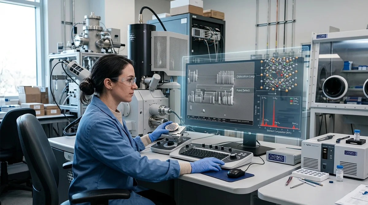
MIT researchers have presented an AI model that helps find and measure atomic defects in materials without destroying the sample. The approach could speed up the development of stronger alloys, more efficient semiconductors, batteries, and solar cells.
How defects are found
In materials science, a defect does not always mean a problem. At the atomic level, such changes in structure are often introduced deliberately to increase mechanical strength, change electrical conductivity, improve heat transfer, or raise energy conversion efficiency. The problem lies elsewhere: after manufacturing, engineers struggle to determine exactly which defects they ended up with and at what concentration. Many existing methods see only part of the picture, and some require cutting or otherwise damaging the sample.
The MIT team tried to solve this by combining machine learning with neutron scattering. The researchers analyzed the vibrational spectra of solid materials, essentially how atoms in a crystal lattice "move" at different frequencies. The model then learned to match these signals to specific types of point defects.
For training, the team assembled a computational dataset of 2,000 semiconductor materials, each with a defective and a defect-free version. The model is built on multihead attention, the same class of architectural ideas used in modern language models.
What the tests showed
After training, the model was fine-tuned and checked against experimental data. The authors write that it could not only recognize individual defects but also quantify their content in real samples. This matters because conventional lab methods often answer either "what kind of defect is this" or "where is it," but do not provide a universal, non-destructive quantitative estimate across several types of structural flaws at once.
According to MIT, the system has already produced several strong results:
- the training set covered 2,000 semiconductor materials;
- the model covers 56 elements of the periodic table;
- it can predict up to six point defects simultaneously;
- sensitivity reaches concentrations of about 0.2 percent;
- the approach was tested on an electronics alloy and on a separate superconducting material.
The authors note that working with mixed signals is what makes the task especially hard. When a single material contains several types of defects, their spectral traces overlap. For classical analysis this quickly turns into guesswork, but the AI was able to extract patterns even where the signals are almost visually indistinguishable.
Where it could be used
The practical value of the work lies in quality control and tuning material properties in production. Manufacturers of semiconductors and other complex materials often use invasive checks on only a small share of output, because such tests are slow, expensive, and destroy the sample. As a result, some decisions about composition and process settings rest on estimates and indirect indicators. More accurate defect diagnostics could cut the number of misses and speed up the search for the desired material characteristics.
The current method has a limitation, though: measuring vibrational spectra with neutrons is too complex and not accessible enough for mass adoption directly on a factory line. So MIT's next step is to transfer the same principle to more common instruments, primarily Raman spectroscopy. The researchers also want to extend the model beyond point defects and teach it to see larger structural features, such as grains and dislocations.
"Defects are a double-edged sword: useful defects are sometimes needed, but too many of them degrade the material's properties," explains MIT professor
Mingda Li.
What this means
This work shows that AI is increasingly becoming not a generator of text or images but a measurement tool for science and industry. If MIT can adapt the approach to more accessible spectroscopy methods, manufacturers will gain a way to understand faster what is happening inside a material and to design chips, electronics, batteries, and energy components more precisely.
Key Questions Answered
How defects are found?
In materials science, a defect does not always mean a problem. At the atomic level, such changes in structure are often introduced deliberately to increase mechanical strength, change electrical conductivity, improve heat transfer, or raise energy conversion efficiency. The problem lies elsewhere: after manufacturing, engineers struggle to determine exactly which defects they ended up with and at what concentration. Many existing methods see only part of the picture, and some require cutting or otherwise damaging the sample. The MIT team tried to solve this by combining mac
What the tests showed?
After training, the model was fine-tuned and checked against experimental data. The authors write that it could not only recognize individual defects but also quantify their content in real samples. This matters because conventional lab methods often answer either "what kind of defect is this" or "where is it," but do not provide a universal, non-destructive quantitative estimate across several types of structural flaws at once. According to MIT, the system has already produced several strong results: the training set covered 2,000 semiconductor materials; the model covers
Where it could be used?
The practical value of the work lies in quality control and tuning material properties in production. Manufacturers of semiconductors and other complex materials often use invasive checks on only a small share of output, because such tests are slow, expensive, and destroy the sample. As a result, some decisions about composition and process settings rest on estimates and indirect indicators. More accurate defect diagnostics could cut the number of misses and speed up the search for the desired material characteristics. The current method has a limitation, though: measuring
Test Frontier LLMs & Autonomous Agents in One Workspace
Run Claude Opus 5.5, GPT-6, Gemini 3.1, and DeepSeek side-by-side in Nomad AI (nomadnet.ai) — unified model routing, deep research, and multimodal workflows under one subscription.
The AI world, distilled — once a week
Seven stories that actually mattered, hand-picked. No noise, no reposts, no press releases.
Done! Check your inbox for a confirmation.