Ahead of GTC 2026, Nvidia teases an optical chip that could rework AI data centers
Ahead of GTC 2026, Nvidia is building anticipation with a promise of a "chip that will shake the world." The most discussed scenario is an announcement of an architecture built on silicon photonics, where data moves between accelerators as light rather than over copper links. If the bet pays off, it would affect more than GPU speed. It would also touch the cost of inference, power consumption and the design of data centers.
AI-processed from Habr AI; edited by Hamidun News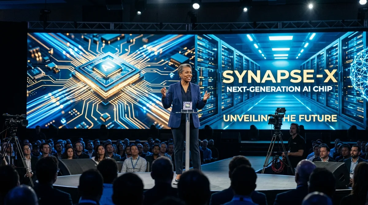
Ahead of Nvidia's GTC 2026 keynote, the market is talking not about another bump in teraflops but about a possible change in how AI chips are connected to one another. The trigger was a line from Jensen Huang about a "chip that will shake the world," delivered before the March 16, 2026 presentation in San Jose.
What Nvidia is promising
On the surface, this looks like a routine product-line refresh. Nvidia has already made Blackwell its current flagship, and at GTC the market expects an official focus on the next generation, Vera Rubin. Blackwell Ultra GB300 already has extreme specs: 288 GB of HBM3e, up to 15 petaflops in FP4, and NVL72 racks that combine dozens of accelerators into a single compute block. These figures matter to the industry, but they do not on their own explain such a loud promise. The comparison with 2016 is no accident: the P100 showing turned out, in hindsight, to be one of the key moments for the modern AI boom.
The intrigue is that Huang did not tie the statement to a specific product. Nvidia usually sets markers in advance: a new architecture, a new rack, a new DGX cluster. This time the market heard a formula with no explanation, and that is why attention shifted from dry specifications to the idea of a breakthrough itself. If Vera Rubin really delivers a multiple-fold increase in memory bandwidth and noticeably lowers the cost of inference, that would already be big news. But the "shake the world" wording hints at a step of a different scale.
Why everyone is looking at optics
The main hypothesis around the announcement is silicon photonics: transferring data between chips with light rather than electrical signals over copper. At the center of these expectations is the Feynman architecture, which is linked to the period after Vera Rubin. The idea is simple: modern GPUs are limited not only by the power of the die itself but also by how fast it exchanges data with neighboring accelerators, memory and networking. The larger the cluster, the more painful the losses on interconnects, the heat and the distance limits become.
"At GTC 2026 we will present a chip that will shake the world."
If Nvidia really shows a working optical interconnect, it will not be a cosmetic improvement but an attempt to remove the main bottleneck of AI infrastructure. Electrical lines lose efficiency as speeds and packing density grow. Optical channels promise more bandwidth per bit, less heat and better scalability. That is why the conversation has suddenly turned not to a 20% performance gain but to rebuilding how large clusters for training and serving models are built in the first place.
What it changes
The move to optics matters not only to engineers counting nanoseconds between chips. It hits data center economics, because today's AI race increasingly runs into energy, cooling and the cost of serving models. The bigger clusters get, the more money goes not to the "brains" themselves but to moving data between them and fighting the heat that this movement creates.
If Nvidia's bet works, the industry could get several practical benefits at once:
- lower energy spent on moving each bit of data;
- less heat output and, as a result, simpler rack cooling;
- the ability to place accelerators farther apart without a sharp loss of speed;
- more flexible layouts for data centers and network infrastructure;
- further reductions in the price of inference for mass-market AI services.
But there is strong skepticism too. Optical interconnects have been promised to the industry for many years, and the road from a lab prototype to a production server rack is always longer than it looks on stage. Nvidia also has a direct incentive to raise expectations: its market capitalization is enormous, competitors such as AMD, Intel, Google and Amazon are investing billions in alternative accelerators, and any presentation instantly becomes a test of leadership. So the main question is not whether a nice slide will be shown, but whether there will be specifics on stage: a working sample, delivery dates and customer names.
What this means
If Nvidia confirms its bet on silicon photonics on March 16, 2026, the news will be bigger than another GPU announcement: it would signal a change in the architecture of AI data centers and a new round of falling compute costs. If the big words hide only a planned upgrade of Blackwell and Vera Rubin, the market will get an important but still evolutionary step, not a technological break. That is why investors, engineers and cloud providers will watch not the slogans but the timelines, prototypes and first customers.
- Nov 1, 2026Local models lose to Opus and Codex: 0.21 on a MacBook versus 1.00 for Codex
- Nov 1, 2026Habr author fine-tunes YOLOv8l on dental X-rays and pushes mAP50 to 0.642
- Nov 1, 2026Voice bots built on LLMs turn to Jev, a fast classifier, for decisions in 200–500 ms
- Nov 1, 2026MoneyGate safety layer blocked all 42 fraudulent requests to local AI models
Key Questions Answered
What Nvidia is promising?
On the surface, this looks like a routine product-line refresh. Nvidia has already made Blackwell its current flagship, and at GTC the market expects an official focus on the next generation, Vera Rubin. Blackwell Ultra GB300 already has extreme specs: 288 GB of HBM3e, up to 15 petaflops in FP4, and NVL72 racks that combine dozens of accelerators into a single compute block. These figures matter to the industry, but they do not on their own explain such a loud promise. The comparison with 2016 is no accident: the P100 showing turned out, in hindsight, to be one of the key m
Why everyone is looking at optics?
The main hypothesis around the announcement is silicon photonics: transferring data between chips with light rather than electrical signals over copper. At the center of these expectations is the Feynman architecture, which is linked to the period after Vera Rubin. The idea is simple: modern GPUs are limited not only by the power of the die itself but also by how fast it exchanges data with neighboring accelerators, memory and networking. The larger the cluster, the more painful the losses on interconnects, the heat and the distance limits become. "At GTC 2026 we will prese
What it changes?
The move to optics matters not only to engineers counting nanoseconds between chips. It hits data center economics, because today's AI race increasingly runs into energy, cooling and the cost of serving models. The bigger clusters get, the more money goes not to the "brains" themselves but to moving data between them and fighting the heat that this movement creates. If Nvidia's bet works, the industry could get several practical benefits at once: lower energy spent on moving each bit of data; less heat output and, as a result, simpler rack cooling; the ability to place acce
Test Frontier LLMs & Autonomous Agents in One Workspace
Run Claude Opus 5.5, GPT-6, Gemini 3.1, and DeepSeek side-by-side in Nomad AI (nomadnet.ai) — unified model routing, deep research, and multimodal workflows under one subscription.
The AI world, distilled — once a week
Seven stories that actually mattered, hand-picked. No noise, no reposts, no press releases.
Done! Check your inbox for a confirmation.