MIT Taught AI to Find Atomic Defects in Materials Without Destroying Samples
MIT demonstrated an AI model for non-destructive material analysis: it identifies atomic defects from vibrational spectra, evaluates their concentration, and…
AI-processed from MIT News; edited by Hamidun News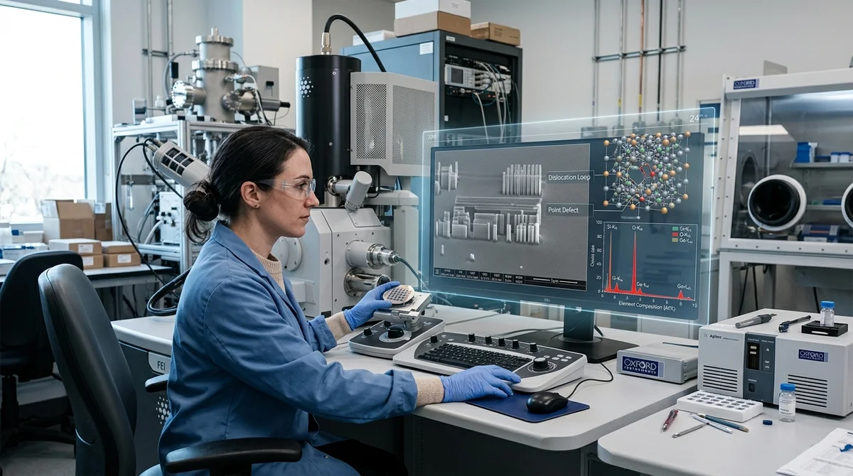
Researchers at MIT have presented an AI model that helps identify and measure atomic defects in materials without destroying the sample. This approach could accelerate the development of stronger alloys, more efficient semiconductors, batteries, and solar cells.
How Defects Are Found
In materials science, a defect doesn't always mean a problem. At the atomic level, such structural changes are often intentionally introduced into a material to increase mechanical strength, modify electrical conductivity, improve heat transfer, or boost energy conversion efficiency. The real problem is different: after production, engineers find it difficult to understand exactly what defects were created and in what concentration. Many existing methods only see part of the picture, and some require cutting or otherwise damaging the sample.
The MIT team tried to solve this problem through a combination of machine learning and neutron scattering. Researchers analyzed vibrational spectra of solid materials—essentially, how atoms in a crystal lattice "move" at different frequencies. The model then learned to match these signals with specific types of point defects. For training, they compiled a computational database of 2000 semiconductor materials: each had a variant with defects and without them. The model's foundation uses a multihead attention mechanism—the same class of architectural ideas used in modern language models.
What Tests Showed
After training, the model was fine-tuned and tested on experimental data. The authors report that it was able not only to recognize individual defects but also to quantitatively assess their content in real samples. This matters because standard laboratory methods often answer either the question "what type of defect is this" or "where is it located," but don't provide a universal, non-destructive quantitative assessment across multiple types of structural defects simultaneously.
According to MIT, the system has already shown several strong results:
- the training database covered 2000 semiconductor materials;
- the model covers 56 elements of the periodic table;
- it can simultaneously predict up to six point defects;
- sensitivity reaches concentrations around 0.2 percent;
- the approach was tested on an electronic alloy and on a separate superconducting material.
The authors particularly note that working with mixed signals makes the task especially difficult. When multiple types of defects are present in one material, their spectral signatures begin to overlap. For classical analysis, this quickly turns into guesswork, but AI was able to extract patterns even where signals are visually almost indistinguishable.
Where It Will Be Applied
The practical value of this work lies in quality control and material property adjustment during manufacturing. Currently, semiconductor and other complex material manufacturers often use invasive testing on only a small fraction of production because such tests are slow, expensive, and destroy the sample. As a result, some decisions about composition and process adjustment are based on estimates and indirect indicators. More accurate defect diagnostics could reduce mistakes and speed up the selection of required material characteristics.
However, the current method has a limitation: neutron measurement of vibrational spectra is too complex and not very accessible for mass implementation directly on a factory line. Therefore, MIT's next step is to transfer the same principle to more common tools, primarily Raman spectroscopy. Researchers also want to expand the model beyond point defects and teach it to see larger structural features, such as grains and dislocations.
"Defects are a double-edged sword: useful defects can be needed, but their excess degrades material properties," explains MIT
Professor Minda Lea.
What This Means
This work demonstrates that AI is increasingly becoming not a generator of text or images, but a measurement tool for science and industry. If MIT can adapt the approach to more accessible spectroscopy methods, manufacturers will gain the ability to more quickly understand what is happening inside a material and more accurately design chips, electronics, batteries, and energy components.
Want to stop reading about AI and start using it?
AI News is a curated feed of AI/tech news. Hamidun Academy teaches you to use AI systematically in your work.