Applied Materials invests $5 billion in semiconductor R&D center for AI
Applied Materials is investing $5 billion to create the EPIC Center, the largest semiconductor technology R&D center in US history. It will open in 2026. The ce
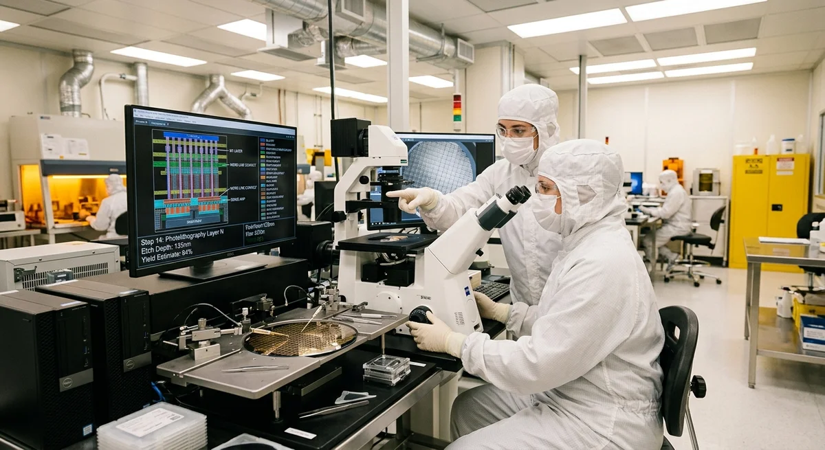
Applied Materials has unveiled EPIC Center — the largest semiconductor technology development center in US history. The $5 billion investment reflects the scale of the challenge: the energy efficiency of AI systems now depends not only on computational power, but also on the efficiency of data movement between logic and memory.
Why the Old R&D Model Doesn't Work
For decades, the semiconductor industry developed chips as a relay race: one team created components and handed them off through integration and manufacturing, only then receiving feedback from engineers in other disciplines. This model worked as long as progress depended on separate, independent steps. But the AI era changed everything. At angstrom scales (billionths of a meter), physics forces tight coupling of all system parts. Material choices impact integration, integration sets design rules, which determine power delivery, and routing sets the thermal budget. System architects cannot wait 10–15 years between technology innovation cycles.
Three Areas of Development
EPIC Center focuses on three interconnected areas:
- Logic — new type transistors (GAA) with improved energy efficiency
- Memory — 3D DRAM with greater capacity at lower power consumption
- Packaging — hybrid bonding and HBM (High-Bandwidth Memory) to bring memory closer to the processor
In logic, Applied Materials is developing gate-all-around (GAA) transistors — three-dimensional devices that increase density without excess power loss. Modern GPUs in development already contain over 300 billion transistors connected by 2000 km of wiring. In memory, the focus is on transitioning from flat structures to 3D DRAM — stacking memory cells vertically to increase capacity in the same die area. In packaging, the key technology is hybrid bonding, which allows components to be connected at density close to on-chip wiring, and high-bandwidth memory (HBM) for fast access to large data volumes.
How EPIC Changes the Process
Unlike the traditional model, EPIC operates on a parallel co-innovation model. Customer engineers work alongside Applied Materials technologists from day one. In a unified secure environment, simulation, testing, process development, and quality control are integrated. Problems that were previously revealed at final stages are now identified and resolved early. The result — a path 2x faster that benefits the entire ecosystem under one roof. Chip manufacturers gain early access to Applied's R&D portfolio, accelerated learning cycles, and technology transfer to manufacturing. Ecosystem partners gain early access to advanced manufacturing technologies.
What This Means
The semiconductor industry is transitioning from sequential to parallel innovation. EPIC Center is an attempt to shorten the time from idea to mass production in conditions where AI demands increasingly energy-efficient and powerful chips. For consumers, this means the next generation of AI accelerators and neural network processors will be developed and deployed faster.