Intel Bets on Chip Packaging — and It Could Bring Billions
While everyone watches nanometers, the real race is heating up around chip packaging. Intel is betting billions on it: EMIB and Foveros technologies allow…
AI-processed from Wired; edited by Hamidun News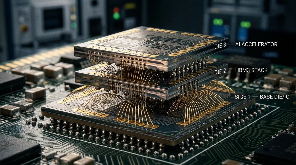
While the public discussion about AI chips revolves around nanometers and transistor counts, the real battle has shifted to a less visible, but far more practical place — chip packaging technology. And Intel, a company many had written off in the race for performance, unexpectedly finds itself at the center of this new competition. Advanced chip packaging is a way to combine multiple separate dies into one package so they work as a single unit.
Instead of increasing the complexity of a single monolithic die (which becomes increasingly expensive and difficult as Moore's Law runs out of steam), engineers have learned to "glue together" specialized blocks — processor cores, memory, accelerators — with minimal signal delays between them. For AI, this changes everything. Modern neural network accelerators, like NVIDIA's GPUs, consume colossal amounts of memory and require extremely high bandwidth between computing blocks and memory.
This is where TSMC's CoWoS technology, which NVIDIA uses in its H100 and H200, provides a competitive advantage — not through a finer process node, but through dense packaging. Intel is moving in the same direction, but with its own advantages. The company is developing two key technologies: EMIB (Embedded Multi-die Interconnect Bridge) — a flat 2.
5D die-to-die connection through silicon bridges, and Foveros — three-dimensional 3D stacking, where dies are literally stacked on top of each other. The combination of both technologies in the Intel Foundry Services lineup opens up possibilities that competitors don't yet have at such a scale. It's important to understand the context: Intel lost its lead in advanced chip manufacturing long ago, ceding it to TSMC.
But packaging is a separate competency. Here, Intel has accumulated decades of experience and infrastructure that isn't easy to copy. This is why the bet on packaging looks strategically sound: it's a way to get back in the game without catching up to TSMC on nanometers.
The market has felt this. The largest technology companies — Microsoft, Google, Amazon — are building their own AI chips through custom design. They all need advanced packaging.
Intel Foundry offers them an alternative to TSMC on American soil — particularly valuable given the geopolitical risks around Taiwan and American subsidies under the CHIPS Act. There are skeptics. Intel has promised technological breakthroughs many times that either delayed or failed to meet expectations.
Foveros has existed for several years, but hasn't yet achieved mass commercial success in the foundry segment. Competitors aren't standing still: TSMC is investing in SoIC and CoWoS, Samsung is developing X-Cube. Nevertheless, the timing looks right.
The AI boom has created an insatiable demand for performance that can no longer be achieved simply by shrinking transistors. Packaging has become the point where engineering exotica turns into an industry standard. And Intel, despite all its problems over the past decade, is at this point with real technologies and real infrastructure.
If the bet pays off, it will be one of the most unexpected turnarounds in the history of the semiconductor industry. If not, Intel will become definitively a niche player. The stakes are high, and this is why the story of "chip packaging" is important far beyond tech circles.
Want to stop reading about AI and start using it?
AI News is a curated feed of AI/tech news. Hamidun Academy teaches you to use AI systematically in your work.