ASML ready for volume production of next-generation lithography systems for AI chips
ASML, the world’s only manufacturer of EUV lithography equipment, has confirmed that its High-NA EUV systems are ready for volume production. These machines…
AI-processed from AI News; edited by Hamidun News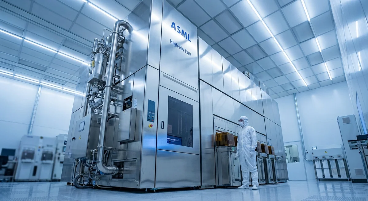
The machine that will determine the shape of artificial intelligence for the next decade has just achieved readiness for mass production. Dutch ASML — the company that holds absolute global monopoly on commercial extreme ultraviolet lithography equipment — has confirmed that its High-NA EUV systems have crossed the threshold from experimental prototypes to full-fledged industrial tools. For the entire semiconductor industry and, as a consequence, for the AI sphere, this event is comparable to the discovery of a new oil field in the midst of an energy crisis.
To understand the scale of what is happening, we need to return to basics. Every modern chip — from processors in smartphones to giant AI accelerators from NVIDIA and AMD — is created using lithography: a process in which light "draws" microscopic circuits on silicon wafers. The shorter the wavelength of this light, the smaller the details and the more transistors that can fit on a single crystal.
ASML's standard EUV systems, operating at a wavelength of 13.5 nanometers, have already become an indispensable tool for manufacturing chips using 7, 5, and 3 nanometer processes. But physics is inexorable: to further reduce element sizes, optics with higher numerical aperture is needed.
This is precisely what High-NA technology provides — the numerical aperture has been increased from 0.33 to 0.55, making it possible to form structures smaller than two nanometers.
Each such system is an engineering marvel weighing around 150 tons and costing, by various estimates, between 350 and 400 million dollars. Transporting a single machine requires several dozen trucks. ASML delivered the first High-NA EUV units to leading chipmakers — Intel, TSMC, Samsung — already in 2024–2025, but until now it has been about research and pilot production lines. The announcement of readiness for mass production means something fundamentally different: the technology has passed checks for stability, reproducibility, and economic viability. Factories can now begin integrating these tools into their production chains not as an experiment, but as a foundation.
For the artificial intelligence industry, this event has direct and immediate significance. Modern large language models and multimodal systems are already hitting the physical limitations of existing chips. Training models at the scale of GPT-5 or Gemini Ultra requires tens of thousands of accelerators consuming megawatts of electricity. The transition to 2 nm processes and below, which becomes possible thanks to High-NA EUV, promises a significant increase in transistor density — meaning more computing power while consuming less energy per unit area of the chip. Simply put, the next generation of AI chips will be able to do more while consuming less, and ASML's lithography systems will be the tool that makes this possible.
The geopolitical context adds additional weight to this news. ASML remains the only company on the planet capable of manufacturing such equipment. The Netherlands, under pressure from the United States, has already restricted exports of advanced lithography systems to China. The readiness of High-NA EUV for mass production reinforces the technological gap between countries that have access to these machines and those that do not. For Beijing, actively investing in its own semiconductor industry, this means that the distance that needs to be overcome is not shrinking but growing. Control over lithography effectively becomes control over the future of the AI industry.
It is also important to note the economic aspect. Given the cost of a single system comparable to the budget of a small unicorn startup, only the largest players can afford High-NA EUV. This further strengthens the oligopoly in advanced chip manufacturing: TSMC, Samsung, and Intel — that is essentially the entire list of companies that will be using this technology at their fabs in the foreseeable future. For AI systems developers, this means maintaining dependence on a narrow circle of silicon suppliers, which can affect the cost and availability of computing resources.
ASML's announcement is not simply a technical milestone. It is the starting signal for a new stage of the semiconductor race, whose results will determine what artificial intelligence models will be like in three to five years. While some companies compete in neural network architectures and the volume of training data, the foundation for all this progress is being laid in the cleanrooms of the Dutch city of Veldhoven — where the most complex machines ever created by humanity are assembled. The countdown to the next technological leap has begun.
Want to stop reading about AI and start using it?
AI News is a curated feed of AI/tech news. Hamidun Academy teaches you to use AI systematically in your work.